POB's research interests are mainly concerned with semiconducting nanomaterial and span interfacial areas of chemistry and materials science. The group is actively involved in precursor design and synthesis, Chemical vapour depositions, Chemical bath depositions, single source approaches to nanocrystals and interfacial deposition.
Synthesis of Quantum Dots, Single Source Precursors and Nanocrystalline Matter
Nanocrystals, tiny fragments of bulk matter have been known since Mesopotamian times (4500 B.C) but have recently received a fillip due the discovery of the effects of quantum confinement and the ability to better characterize and study their properties. By virtue of their diameters being between 1 and 20 nanometers, the particulates possess a high specific surface area, compared to other materials and are highly useful catalyst. Upon being turned into nanocrystals, all materials become highly reactive and acquire entirely new set of properties.(See recent lectures, How small is important for more) For example, nanocrystalline gold is no longer noble, nor does it possess the familiar “golden yellow” lustre. Semiconductors in the form of nanocrystals, have higher band gap and turning a semiconductor into nanocrystals of different diamaters has emerged as a useful method for tuning band gap.
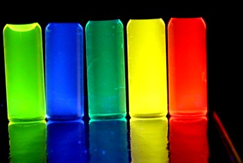 |  |
| Flourescence from nanocrystals of different diameters. |
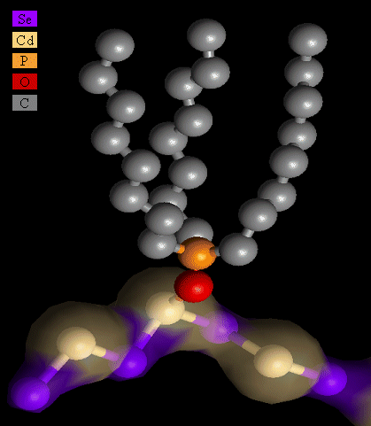
Structure of the TOPO ligand on CdSe nanocrystal as ascertained by Extended X-ray Absorption Fine Structure studies |
POB has been keenly interested in the synthesis and properties of semiconductor and other nanocrystals. Active research from POB group has been instrumental in developing new benign routes to nanocrystalline material. Many of the routes rely on single source precursors and have proved valuble in replacing pyrophoric methods that have previously been used to generate nanocrystals. The potential use of several families of organometallic compounds as single source precursors have been investigated by this group. A few recent results are pictorially summarized below.
 |
 |
 |
 |
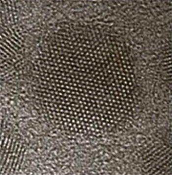
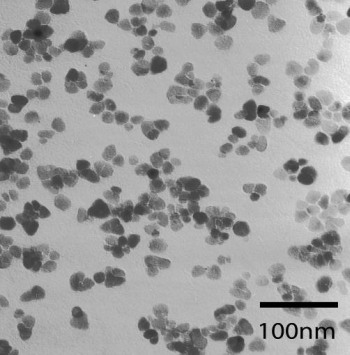
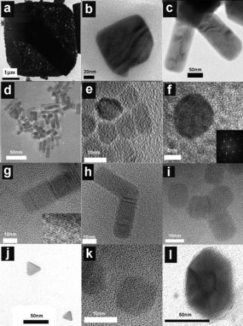
| High resolution Transmission electron microscopic image of a CdSe nanocrystal |
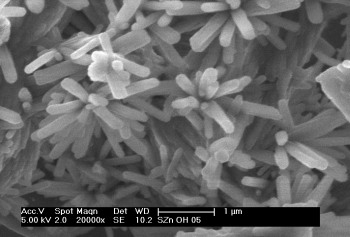
Transmision electron microscopic image of ZnO nanocrystals obtained by decomposition of zinc ketoacidoximate |
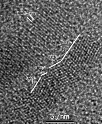
High resolution Transmission electron microscopic image of a CdS nanorod. The cubic and hexagonal domains are marked with C and H. |
Transmision electron microscopic image of CoP nanorods, obtained by prolonged thermolysis of Co(acac)2 in TOPO. |
 |
 |
 |
 |
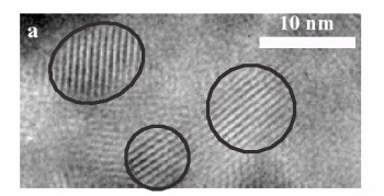
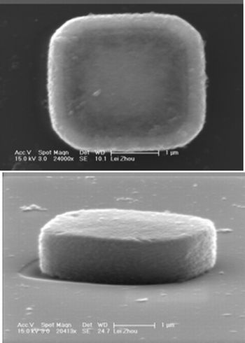
| High resolution Transmission electron microscopic image of EuS nanocrystals obtained by irradiation of Eu dithiocarbamate. |
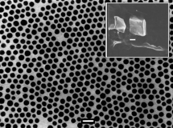
2D lattice of octadecylamine/TOPO capped gold, bar = 20 nm. Inset is a SEM image of cubic colloidal crystal prepared from octadecylamine/ TOPO capped gold nanoparticles. |
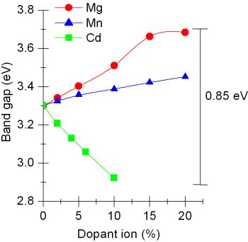
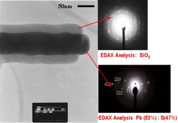
Transmission electron microscopic image of PbS nanocrystals of different shapes synthesized using single-source precursors and a household pressure cooker | Band-gap variation of ZnO nanocrystals brought about by doping with different ions |
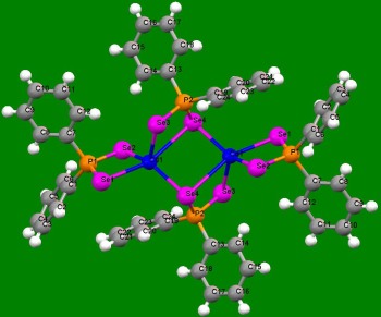
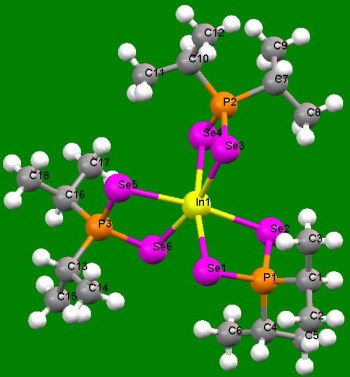
The development of easier and more viable synthetic routes to coordination complexes, especially those involving sulphur, selenium and phosphorous has been a subject of interest. Recent examples include the discovery of easy synthesis routes to metal-selenophosphinate complexes of form [M(R 2PSe2)n] (M = Zn(II), Cd(II), Pb(II), In(III), Ga(III), Cu(I), Bi(III), Ni(II); R = iPr, Ph).
 |
 |
| Crystal structure of Cd selenophosphinate complex. |
Crystal structure of In selenophosphinate complex. |
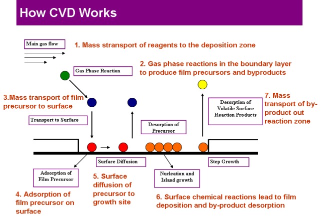
Chemical vapour deposition
New synthetic routes to thin films of oxides and chalcogenides have been developed by chemical vapour deposition. The group is equipped to carry out traditional CVD, aerosol assisted chemical vapour deposition as well as low pressure chemical vapour deposition. Using the above CVD methods, precursors that have limited solubility or low vapour pressure (or volatility) can still be used to grow thin films. Recently, CVD based methods have also been used to catalytically grow nanoscopic material.
 |
 |
 |
 |
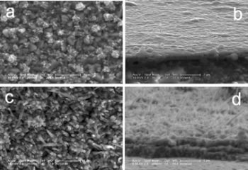
| Scanning electron microscopic image of In2S3 films grown on glass substrate. |
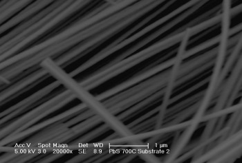
High resolution transmission electron microscopic image of In2S3 rods. |
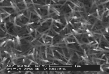
Scanning electron microscopic image of silica coated PbS nanorods grown on glass substrates impregnated with Au nanoparticles. |
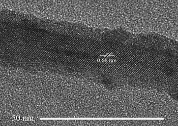
Transmission electron microscopic image of silica coated PbS nanorods. |
Chemical bath deposition, Liquid Phase deposition and Crystal growth
Chemical bath deposition, which involves careful control of precipitation in a mixture of chemical (or bath) enjoys many advantages over traditional deposition methods. Advantages include scalability and energy efficiency. The above quest is inspired by the recognition of the need to reduce the environmental impact of material processing as far as possible. Recent successes include the growth of CdS films from acidic medium.
Another method of deposition that has been of interest involves deposition at the interface of two liquids. In this method, metal ions in organic medium are held in contact with an aqueous solution containing anionic species such as S2-. The deposits are confined to the interface by forces naturally present at the interface of liquids. This method of interfacial deposition shares all the advantages of CBD and is potentially even more straightforward, because it doesn't rely on complexing agents to slowly release the ions into solution.
 |
 |
 |
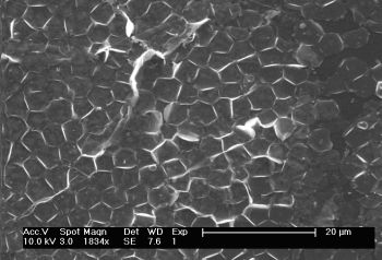 |
| Scanning electron microscopic image of TiO2 uniform crystallites grown by CBD method. |
Scanning electron microscopic image of Bi2S3 films grown by CBD method. |
Scanning electron microscopic image of interfacially grown ZnO film. |
Scanning electron microscopic image of interfacially grown ZnS film. |
For further information please look through recent publications and lectures
|